HCF4094YM013TR
Original price was: $0.6100.$0.5900Current price is: $0.5900. & Free Shipping
roduct overview
Description
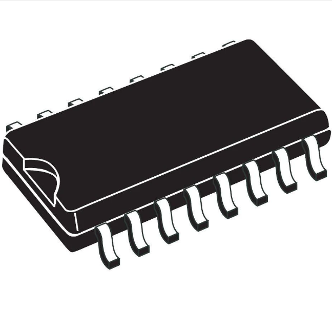
The HCF4094 is a monolithic integrated circuit fabricated in metal oxide semiconductor technology available in an SO-16 package. The HCF4094 is an 8-stage, serial shift register having a storage latch associated with each stage for strobing data from the serial input to parallel buffered 3-state outputs. The parallel outputs may be connected directly to common bus lines. Data are shifted on positive clock transition. The data in each shift register stage are transferred to the storage register when the STROBE input is high. Data in the storage register appear at the outputs whenever the OUTPUT-ENABLE signal is high. Two serial outputs are available for cascading a number of HCF4094 devices. Data are available at the QSserial output terminal on positive clock edges to allow for high speed operation in a cascaded system in which the clock rise time is fast. The same serial information, available at the Q’Sterminal on the next negative clock edge, provides a means for cascading HCF4094 devices when the clock rise time is slow.
Free shipping on orders over $50!
- Satisfaction Guaranteed
- No Hassle Refunds
- Secure Payments
Description
Product overview
Description
The HCF4094 is a monolithic integrated circuit fabricated in metal oxide semiconductor technology available in an SO-16 package. The HCF4094 is an 8-stage, serial shift register having a storage latch associated with each stage for strobing data from the serial input to parallel buffered 3-state outputs. The parallel outputs may be connected directly to common bus lines. Data are shifted on positive clock transition. The data in each shift register stage are transferred to the storage register when the STROBE input is high. Data in the storage register appear at the outputs whenever the OUTPUT-ENABLE signal is high. Two serial outputs are available for cascading a number of HCF4094 devices. Data are available at the QSserial output terminal on positive clock edges to allow for high speed operation in a cascaded system in which the clock rise time is fast. The same serial information, available at the Q’Sterminal on the next negative clock edge, provides a means for cascading HCF4094 devices when the clock rise time is slow.
All features
3- state parallel outputs for connection to common bus
Separate serial outputs synchronous to both positive and negative clock edges for cascading
Medium speed operation 5 MHz at 10 V
Quiescent current specified up to 20 V
Standardized symmetrical output characteristics
5 V, 10 V, and 15 V parametric ratings
Input leakage current II= 100 nA (max.) at VDD= 18 V, TA= 25 °C
100% tested for quiescent current
ESD performance
HBM: 1 kV
MM: 200 V
CDM: 1 kV
 R6006KND4TL1
Reviews
There are no reviews yet.